Image formation and element analysis with a SEM-EDS system
On the page about the
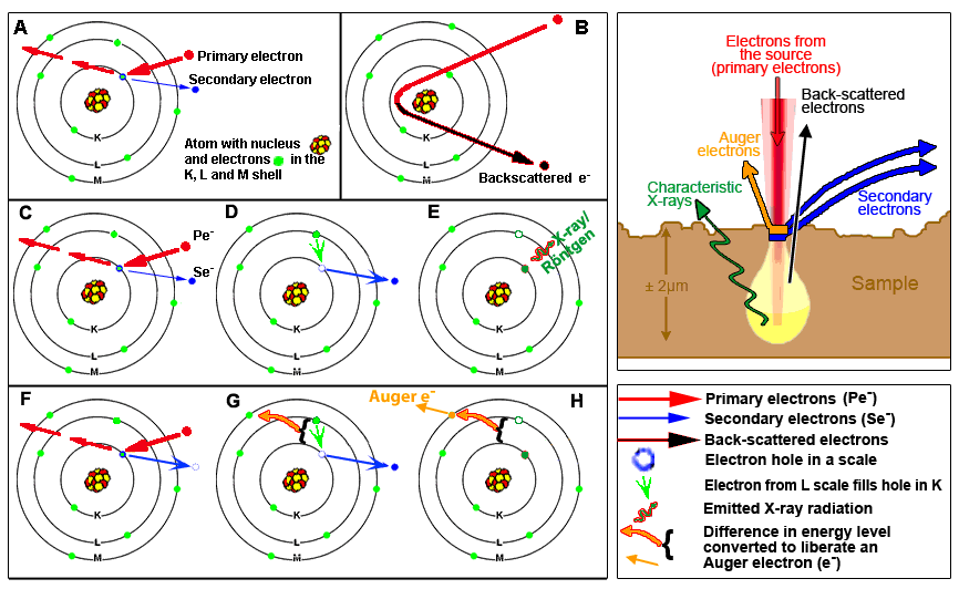
principle of a scanning electron microscope(SEM), we saw that the sample in this instrument is bombarded by an electron beam in order to obtain a detailed topographical image of the surface of the sample from the ejected electrons (secondary electrons, see figure
A here below). Besides, there are scanning electron microscopes which are equipped with
EDS (Energy Dispersed Spectroscopy) or EDAX (Energy-Dispersed Analysis of X-rays) detectors that capture the emitted X-ray (figure
C,
D and
E). With such intruments, like the one shown here below, it is possible to determine
which elements are present in the surface layer of the sample (at a depth in the micrometer range) and
where these elements are present ("mapping technique"). This particular microscope also allows one to capture directly reflected electrons, the so-called
back scattered electrons (figure
B), from which one can obtain a global appreciation whether one or several elements are present in the surface layer of the sample. Also the so-called Auger electrons, which are emitted just under the surface (
F,
G en
H), provide information about the nature of the atoms in the sample.
| Secondary emission in Scanning Electron Microscopy |
 |
A: The bombarding electrons (=primary electrons) can penetrate in the electron shells of the atoms composing the surface of the sample. The energy (negative charge, mass, velocity) of these incident electrons can be converted to eject local electrons, so-called secondary electrons, from the shells of the atoms in the surface of the specimen. This information cab ne utilized to reconstruct a detailed topographical image of the sample (SEI = Secondary Electrons Imaging). The final image looks like a shadow-cast photograph of the surface of the sample. This record of the morphology is the best-known application of a scanning electron microscope.
B: Primary electron can also be reflected by atoms at about 10-100 nanometer depth at the surface. These so-called "back-scatter" conserve their energy at incidence, but their direction of propagation has been modified upon interaction. One can obtain a rough representation wheter the surfaceof the sample is constitued of a single or multiple elements.
C, D, E: at the surface of the sample electrons in the deeper electron shells (shell K in C) can be ejected by primary electrons (Pe- indicated in red), resulting in an electron hole. When this lower-shell position is filled by an electron from a higher shell (green arrow in D) energy is released. This can be as light (photons; the phenomenon is also called cathode luminescence) or as X-ray. Because each element emits an own characteristic energy value, the elements present in the micrometer range depth of the sample can be determined. See example here below.
F, G, H: another phenomenon is that the energy released upon filling a hole in the K shell by an electron from the L shell is used to expulse an electron from the external M shell: a so-called Auger electron. The released energy is characteristic for the type of atom. Auger electrons are produced in the outermost surface layer (at nanometer depth) of the sample.
|
A Scanning Electron Microscope (SEM) with Energy Dispersed Spectroscopy (EDS) detection
How does an EDS microscope look like
The scanning electron microscope shown here below has as particularity that it is equipped with an X-ray detector for
EDS (Energy Dispersed Spectroscopy) or
EDAX (Energy-Dispersed Analysis of X-rays) analysis of elements. One can also obtain a "normal" topographical SEM image from the signal from the
secondary emission electrons as well as a global view of the diversity of elements present in the sample surface from the
"back-scatter electrons". The EDS technique is utlilized on both biological specimen and material science. Examples of applications of EDS are the detection of elements in scales of fishes living under various physiological conditions and the screening of coatings used in solar cells.
| Scanning electron microscope equipped with an Energy Disperse Spectroscopy detector |
|
|
Parts of and around the EDS- scanning electron microscope
1 Kolom
2 Liquid nitrogen (cooling dewart)
3 EDS detector
4 SEI detector
5 Height (z) adjustment of the sample stage
6 x-y navigation of the sample
7 Pre-vacuum chamber
8 Insertion rod
9Sample holder[
10 Conductive tape
11 Sample support block
12 Vacuum device
13 Control panel
14Monitor for the SEM images
15Monitor for the applications
16 Vacuum gauge
17 Monitor of infrared camera (view of SEM chamber)
18 Cooling water
19 Power supply
20 Applications and results of the EDS
|
The employment of the various parts of the microscope
The sample is fixed with conductive tape (10) on a metallic sample block (11) (see close-up picture of such block with test samples here below). Non-conductive specimen are coated with a nanometer thin-layer of metal to facilitate emission and flow of electron in the surface. The metal block is crewed on a sample holder (9) and positioned in the pre-vacuum chamber (7), an intermediate chamber with a front and a rear lid. This chamber acts as a lock. When the vacuum in this space islow enough the shutter to the high vacuum (lowest pressure) is opened and the object is shifted with a long rod (8) into the object chamber on a rails just under the column (1). In orde to ease the positioning a one can observe the innerview of the object chamber with an infra red camera. The object chamber is the place where the sample is irradiated by the electron beam. The position of the sample stage can be adjusted in height (z-navigation 5) and horizontally (x-y navigation; 6). The topografical scanning electron imaging requires a secundary electrons detector (4), like in a normal SEM (see webpage on principle): there is a control panel (13), a monitor for the operation of the device (15) and one showing the SE images (14). A separate EDS detector (3) allows one to capture the X-ray scanning and there is another back-scattered electron detector. In this chamber in the heart of the electron microscope the vacuum is extremely low: 10-6mBar (thus 1:1.000.000.000 the normal atmospheric pressure!; vacuum display = 16; around the electron gun the vacuum is even two orders of magnitude lower!). The need for such extreme vacuum is that collision of bombarding electrons from the beam with gas molecules in the column would result in heat production. Cooling (18) and supply of electric power (19) are required in order to maitain this extreme vacuum.
The Jeol microscope presented here belongs to the Institute for Molecules and Materials (IMM), but it is hosted at the Department of General Instrumentation (here at work, technician Geert-Jan Janssen).
|
Example of EDS results
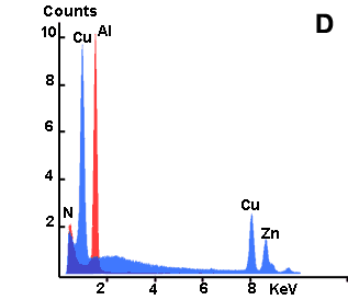
Here below an example is shown of the analysis of test samples in which characteristics X-ray frequencies for Zinc (Zn), Copper (Cu) and Aluminium (Al) are detected as dinstinct peaks. Besides, the signal originating from various parts of the sample has been accumulated over a longer period in order to form a kind of map of the location of single elements (mapping technique). In this example the procedure has been carried out for copper. A corresponding SE image shows the 2D topography of the sample surface.
 |
 |
 |
 |
Element mapping using an EDS SEM:
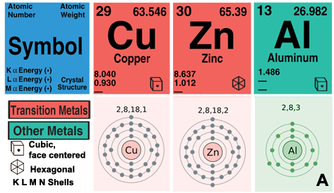
- A. Data on atomic number, atome mass and the distribution of electrons in K, L and M shells for the elements Zinc (Zn), Copper (Cu) and Aluminium (Al). More here about in an interactive Periodical System and an interactive table of electron shells on other websites.
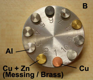
- B. Test sample with various metals, constitued either of single elements or of alloys, like here brass that contains both Copper and Zinc.
- C. Topographical view of the brass disc from abovetest sample obtained by secondary electron imaging (SEI), corresponding Mapping view for copper (Zinc mapping is not shown here) obtained by EDS detection, and overlay view of both signal in false color for a more accurate comparison.
- D. X-ray leaks for Zinc (Zn), Copper (Cu) and Aluminium (Al) detected by EDS.
|
Further reading: Wikipedia page on
electron microscopy and specifically the
SEM, and references herein
